


SMT Assembly Process Explained: How Custom PCBs Are Built
Surface Mount Technology (SMT) is the dominant method used in modern custom PCB assembly. It allows for smaller component sizes, higher board density, and faster automated production compared to older through-hole methods. If you are working with a contract manufacturer on a custom build, your boards will almost certainly go through an SMT line.
Understanding how the SMT assembly process works helps you write better specs, catch design issues before they reach production, and have more informed conversations with your manufacturing partner.
Step 1: Solder Paste Printing
The process starts with applying solder paste to the bare PCB. A stainless steel stencil, cut to match your board’s pad locations, is aligned over the board. A squeegee pushes solder paste through the stencil openings, depositing a precise amount of paste on each pad.
Paste volume and consistency matter here. Too little solder and joints will be cold or open. Too much and you risk bridging between adjacent pads, which is especially problematic on fine-pitch components. Modern lines use 3D solder paste inspection (SPI) immediately after printing to catch issues before any components are placed.
Step 2: Automated Component Placement
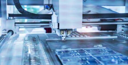
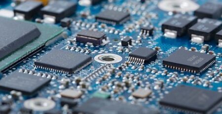
Pick-and-place machines retrieve components from reels, trays, or tubes and place them onto the solder-pasted pads at high speed and with high precision. Modern machines can place thousands of components per hour and handle a wide range of package types, including:
- Passive components (resistors, capacitors) down to 0201 and smaller
- Integrated circuits in QFP, QFN, and BGA packages
- Fine-pitch devices requiring sub-millimeter placement accuracy
- Large connectors and shielding cans
Component placement programs are generated from your CAD data and BOM. Accurate pick-and-place files are critical for a smooth setup and reduce the chance of placement errors or missing parts.
Step 3: Reflow Soldering
After placement, the board travels through a reflow oven. The oven follows a precise thermal profile, gradually raising the board temperature to melt the solder paste, then cooling it in a controlled manner to form solid solder joints.
The reflow profile is tuned to the solder alloy, board thickness, and component thermal mass. SVTronics uses nitrogen-purged reflow processing, which reduces oxidation during soldering and improves joint quality, particularly for fine-pitch and lead-free assemblies.
Step 4: Automated Optical Inspection (AOI)
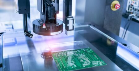
After reflow, boards go through automated optical inspection. AOI systems use high-resolution cameras and lighting from multiple angles to check every solder joint and component placement against your specifications. Common defects caught at this stage include:
- Missing or misaligned components
- Solder bridges between adjacent pads
- Insufficient or excessive solder
- Lifted leads on QFP packages
- Wrong polarity on diodes and electrolytic capacitors
AOI is a non-destructive, 100-percent inspection method. Any board that fails AOI is flagged for manual review before moving further down the line.
Step 5: X-Ray Inspection for Hidden Joints
Some components, particularly BGAs and other bottom-termination packages, cannot be visually inspected after reflow because the solder joints are hidden under the package body. X-ray inspection allows technicians to view the solder ball connections and identify voids, bridges, or incomplete reflow without damaging the board.
X-ray inspection is especially important on custom PCBs with high-density packages or when your application has strict reliability requirements.
Step 6: Through-Hole and Secondary Operations
Many custom boards combine SMT with through-hole components such as connectors, large capacitors, or transformers. These are typically inserted after SMT reflow and soldered using wave soldering or selective soldering equipment. Mechanical assembly, conformal coating, and box build operations may follow depending on your build requirements.
For a detailed comparison of SMT and through-hole methods, see our article on through-hole vs. SMT assembly.
What This Means for Your Custom PCB Build
The SMT assembly process is well-established and highly automated, but it is only as good as the inputs you provide. Clean Gerber files, an accurate BOM, complete placement data, and a well-reviewed stackup all contribute directly to a successful first article. Working with a contract manufacturer that performs DFM review before production starts helps catch issues that would otherwise surface as rework or scrap.
Learn more about SVTronics’ full capabilities on our Custom PCB Manufacturing and Assembly page, or read our overview of custom PCB assembly vs. PCB fabrication to understand where the SMT process fits in the broader production flow.




Leave a Reply