What Is a PCB and How Does It Work?
In today’s digital world, nearly every electronic device—from smartphones and laptops to medical equipment and vehicles—relies on a component that often goes unnoticed: the printed circuit board, or PCB. But what is a printed circuit board, and how does it work?
At SVTronics, understanding how PCBs function is essential to appreciating the complexity and importance of printed circuit board assembly in modern technology. Here’s a straightforward guide to the basics.
What Is a Printed Circuit Board?
A printed circuit board (PCB) is the physical platform for supporting and connecting electronic components. Made primarily from a non-conductive material such as fiberglass (laminate), a PCB features thin layers of copper foil that form the conductive pathways for electricity to flow between components.
These boards are often called circuit cards, printed wiring boards, or simply circuit boards. Regardless of what you call them, they’re found in almost every electronic product today—from simple toys to advanced medical and aerospace systems.
The Role of a PCB in Electronics
The function of a PCB is twofold:
- Mechanical Support: It is a platform for mounting electronic components like resistors, capacitors, and microchips.
- Electrical Connection: It routes electrical signals through copper pathways (traces) to allow different components to communicate and operate as a single system.
The copper pathways are carefully etched into the board based on the device’s circuit design, making each PCB a custom-built solution for a specific product.
Types of PCBs: Single-Sided, Double-Sided, and Multilayer
PCBs come in several configurations, depending on their complexity and application:
Single-Sided PCB
- Definition: A board with circuitry only on one side.
- Common Uses: Simple consumer electronics like calculators or remote controls.
- Advantages: Cost-effective, easy to design and manufacture.
Double-Sided PCB
- Definition: Circuitry exists on the board’s top and bottom layers.
- Common Uses: Power supplies, LED systems, and more complex devices.
- Advantages: Allows for more compact design and increased circuit density.
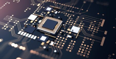
Multilayer PCB
- Definition: Contains three or more layers of conductive circuitry, sandwiched between insulating layers.
- Common Uses: Smartphones, medical equipment, aerospace, and defense systems.
- Advantages: High functionality in compact form, better signal integrity, reduced electromagnetic interference.
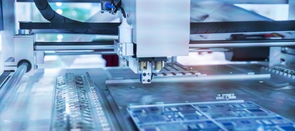
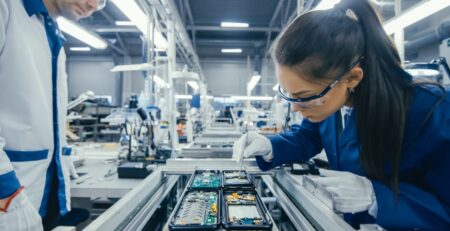
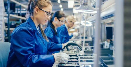
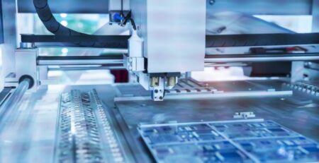
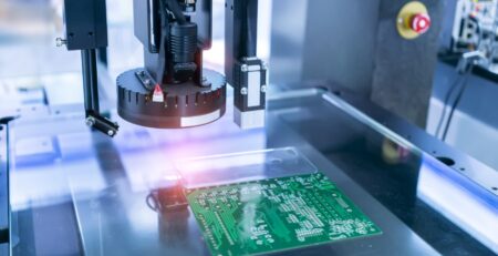
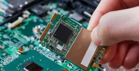
How Printed Circuit Board Assembly Works
Once the bare PCB is fabricated, it undergoes printed circuit board assembly (PCBA), which attaches electronic components to the board. This is typically done in two ways:
Through-Hole Technology (PTH)
- Components are placed into pre-drilled holes and soldered from the opposite side.
- It offers strong mechanical bonds and is commonly used in high-stress applications.
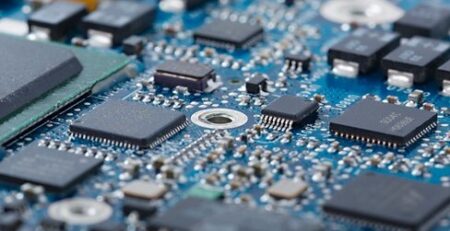
Surface Mount Technology (SMT)
- Components are soldered directly onto the surface of the board.
- More efficient and compact; used in the majority of modern electronics.
These methods can be used individually or combined, depending on the requirements of the product.
Why PCBs Matter
PCBs are the backbone of all modern electronics. Without them, electronic components would not be able to communicate or work together efficiently. As products become smaller and more complex, the demand for innovative printed circuit board assembly solutions grows.
At SVTronics, we specialize in custom PCB assembly services for industries where performance and precision matter—medical, aerospace, defense, automotive, and more.
Start Your Next PCB Project with SVTronics
So, what is a printed circuit board? It’s more than just a green slab with lines—it’s the nervous system of every electronic product. And with the right design and assembly partner, your PCB can bring your innovations to life.
Ready to start your next PCB project? Contact SVTronics today to learn how our team can support your PCB assembly needs—from prototype to production.


Leave a Reply