Multilayer PCBs Explained: Why More Layers Mean More Power
As electronic devices become smaller and more powerful, the need for advanced printed circuit board (PCB) designs has grown exponentially. Enter the multilayer PCB—a compact yet highly functional solution that allows manufacturers to pack more capability into tighter spaces. In this blog, we’ll explore what makes a multilayer PCB unique, how it evolved from single-layer boards, and why it’s a game-changer in modern PCB assembly.
The Evolution from Single-Layer to Multilayer PCBs
In the early days of electronics, PCBs were typically single-sided, meaning all circuitry was confined to one side of the board. This design was simple and cost-effective but limited in terms of functionality and component density.
By the 1970s, the introduction of double-sided boards—where copper traces could be placed on both sides—revolutionized design flexibility. However, as technology continued to advance, double-sided boards still weren’t enough to meet the demands of high-performance applications. This led to the development of multilayer PCBs, which consist of three or more conductive layers stacked together and separated by insulating material.
How Does Multilayer PCB Layering Work?
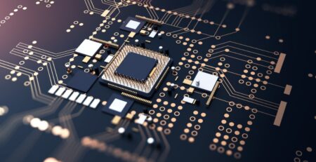
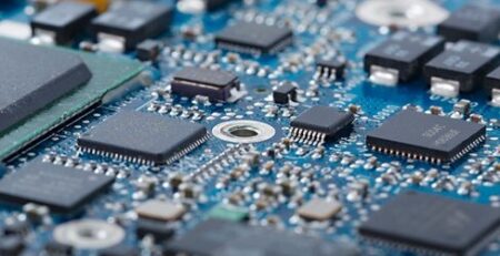
Multilayer PCBs are built by stacking alternating layers of conductive copper and insulating material (laminate and prepreg). These layers are pressed and bonded together through a heat and pressure process, creating a single, unified board structure.
The internal layers are carefully designed to route complex signals while reducing electromagnetic interference (EMI) and maintaining signal integrity. Vias—small plated holes—are used to connect traces between layers, allowing for highly intricate and compact designs.
Advantages of Multilayer PCBs
- Higher Functionality: The additional layers allow for more complex circuits and higher component density.
- Compact Design: Multiple layers reduce the need for larger single-layer boards, enabling sleek and lightweight devices.
- Improved Signal Quality: Layering decreases EMI and cross-talk, boosting overall performance.
- Durability: The bonded structure provides added strength and stability compared to single or double-layer boards.
Applications of Multilayer PCBs
Multilayer PCBs are commonly used in applications where performance and space efficiency are essential. These include smartphones, medical devices, aerospace systems, automotive electronics, and high-speed computing devices.
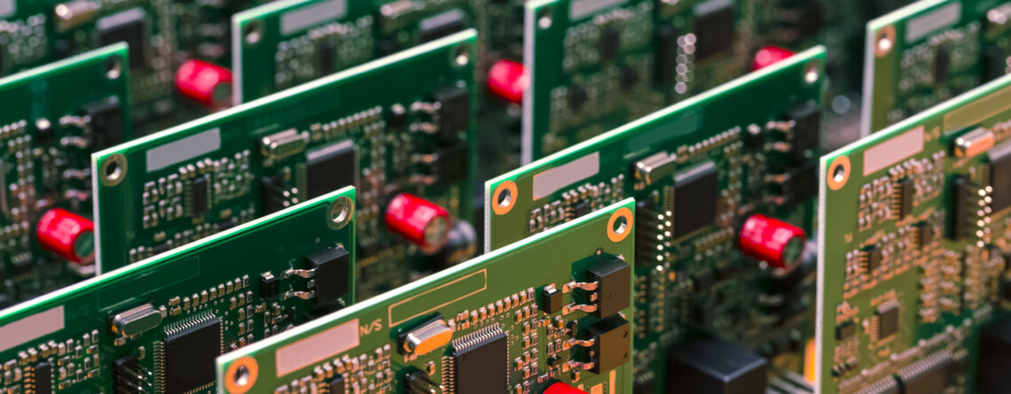
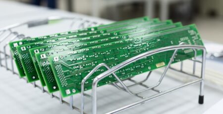
SVTronics: Your Multilayer PCB Assembly Partner
At SVTronics, we specialize in advanced PCB assembly, including multilayer PCB production for industries that require precision and high reliability. Our expertise in handling complex designs and our state-of-the-art manufacturing facility in Plano, Texas, make us the trusted partner for multilayer PCB assembly.
Final Thoughts
The multilayer PCB has transformed the electronics industry by enabling more powerful devices in smaller, more efficient packages. Whether you need a simple prototype or a high-density, multi-layer design, SVTronics has the tools, technology, and experience to bring your vision to life.
SVTronics is a U.S.-based PCB manufacturer. Contact us today for all your PCB manufacturing needs.


Leave a Reply