Ensuring that your PCB design is up to par is critical to the success of your electronic device. Failure to do so can result in many problems including poor electrical performance, shorts, and circuit failures.

To help you avoid these pitfalls and ensure that your design can withstand the rigors of real-world use, we’ve compiled a list of answers to some of the most common PCB design questions.


What Is PCB Design?

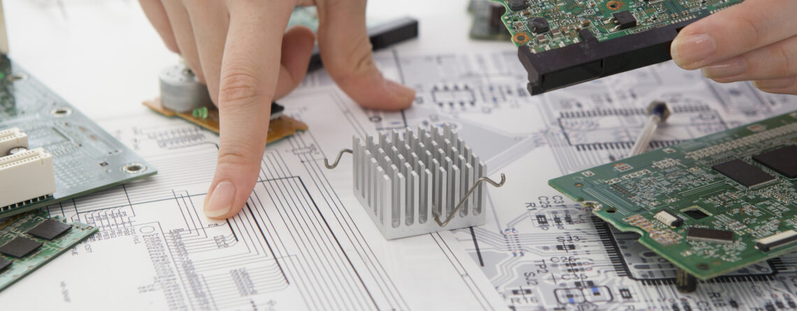
PCB design is an essential part of PCB assembly that’s needed for creating functional, reliable, and safe electronic products. It encompasses the process of drawing up and preparing to assemble a printed circuit board, which is used to support and connect electronic components. The design process includes:

  • Creating a schematic
  • Selecting the appropriate PCB materials
  • Laying out the components on the board

What Is a PCB Made Of?

PCBs are made up of several materials, the most common of which is FR-4. This is a glass-reinforced epoxy laminate with excellent dielectric (nonconductive) properties and is resistant to heat and flame.

Other PCB materials used in PCB manufacturing include a substrate, copper, solder mask, and silkscreen. These materials are chosen based on the specific performance requirements of the PCB and the application it will be used in.

A substrate is a material (typically fiberglass) that the traces and components of PCBs are bonded to. It provides mechanical support and determines the dielectric properties of the PCB.

Copper is used for creating circuit tracks on the PCB. It is a good conductor of electricity and has a low resistance, making it ideal for carrying signals between electronic components. Typically, the thickness of copper needed for a particular board is determined by the amount of current the tracks must carry.

A solder mask is a layer of insulating material applied to the PCB to protect copper traces from short circuits, corrosion, and other forms of damage. It also makes it easier to solder components onto the PCB, reducing the risk of solder beads forming on the surface of the board during manufacturing.

Silkscreen is a printing process used to apply labels and other markings to the PCB. These markings help identify different components and their functions.

Why Is Copper Used?

Copper is an excellent conductor of electricity and has a low resistance. This makes it ideal for carrying signals between electronic components. Furthermore, its heat conductivity properties make it ideal for reducing the risk of damage and component failures due to overheating.

While other materials such as aluminum may have similar properties, copper is the preferred choice for PCBs due to its lower cost, availability, and even heat distribution.

What Components Do All PCBs Need?

No matter the purpose of the PCB, every design will need to incorporate certain components. These include:

  • Resistors: Used to control current flow in a circuit and protect against voltage spikes.
  • Capacitors: Used to store electrical energy and smooth out voltage fluctuations.
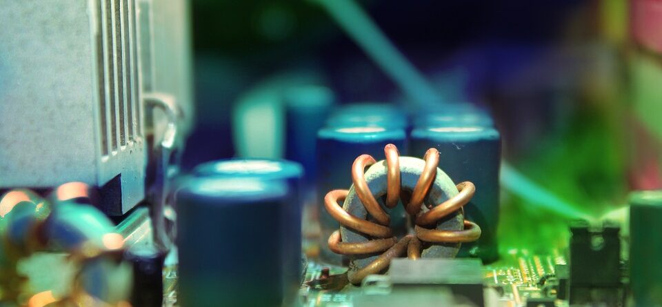
  • Inductors: Used to store energy in the form of a magnetic field and control the flow of current.
  • Potentiometers: Used to control the voltage in a circuit by acting as a variable resistor.
  • Transformers: Used to transfer electrical energy between two circuits by converting the voltage levels.
  • Diodes: Used to allow current to flow in one direction only and protect against voltage spikes.
  • Translators: Used to convert signals from one voltage level to another.
  • Silicon-Controlled Rectifier: Used to control the flow of current in a circuit by acting as a switch.
  • Integrated Circuits: Used to perform complex tasks such as amplifying signals or storing data.
  • Crystal Oscillators: Used to generate a stable clock signal for electronic devices.
  • Switches & Relays: Used to control the flow of current in a circuit by acting as an electronically controlled switch.
  • Sensors: Used to detect changes in the environment and convert them into electrical signals.

What Equipment Is Used in PCB Design?

Knowing the parts of a PCB is only half the battle — to design and manufacture a functioning board, you’ll need the right tools and equipment. Essential pieces of equipment used in PCB design include stencils, a soldering machine, computer-aided design software (CAD), a Gerber file, and an Excellon file.

Stencils are the templates used to apply the solder paste to the PCB. Stencils ensure that the solder paste is applied precisely where it should be so that components are soldered onto the PCB with perfect alignment.

A soldering machine is used to heat the solder so that it can flow into the space between the component and the PCB, making a secure connection.

CAD software is used to design the PCB layout. This software allows engineers and designers to place components, connect traces, and test the board in a virtual environment before sending it to manufacturing.

The Gerber file is an instruction set that tells the manufacturer how to produce the PCB. These ASCII vector format files contain all of the information about the PCB layout, including the location of the components and traces.

The Excellon file is used to drill the holes in the PCB. This file contains the coordinates of where the holes need to be drilled as well as the size of each one.

To design a PCB that works properly in real-world scenarios, you will need all of these essential pieces of equipment. Without them, it would be impossible to create a functioning board.


What Is a Return Current?

A return current is the path of least resistance for the current to flow back to the power source. This is important in PCB design because it prevents inductive coupling, which can cause voltage spikes and damage components. When designing your PCB layout, the return current can be optimized by using adjacent reference planes to create a low-impedance path.

Consider Working With an EMS Partner

Effective PCB design is essential to the success of your electronics project. While it can be confusing to understand the many aspects of PCB design, working with an experienced electronic manufacturing services (EMS) partner can make the process much easier. An EMS partner can help you select the right components for your project, design a PCB layout that meets your needs, and manufacture the board to your specifications.

For more answers to PCB questions that will ensure a successful outcome for your electronics project, here are the factors for PCB design and layout to consider when working with an EMS partner.