The Full Lifecycle of a Printed Circuit Board: From Design to Assembly
Printed circuit boards (PCBs) are the backbone of nearly every electronic device we rely on today, from smartphones and smartwatches to medical devices and aerospace equipment. But many people don’t see the intricate and highly coordinated process it takes to bring a PCB from initial concept to a fully assembled, functioning product.
At SVTronics, we specialize in managing the full lifecycle of a PCB, delivering end-to-end electronic manufacturing services that ensure high performance, quality, and speed to market. Here’s a look at what that lifecycle involves.
1. Design and Engineering
The process begins with circuit design, usually created by OEMs or design engineers using CAD tools. The goal is to define how electronic components interact, which connections are required, and how signals flow across the board. This step also includes selecting materials, determining board size, and optimizing layout for electrical performance and manufacturability.
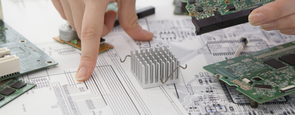
2. Prototyping and Layout Validation
Once the schematic is finalized, a prototype PCB is developed. This test version allows engineers to validate the board’s electrical performance, physical design, and manufacturability. Gerber or ODB++ files are typically used to communicate the design to fabricators. Any design flaws are identified and corrected at this stage before full-scale manufacturing begins.
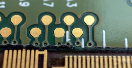
3. PCB Fabrication
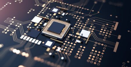
The fabrication process transforms design files into a physical board. It involves layering copper foil, insulating laminate, etching conductive pathways, and drilling vias and component holes. For multilayer boards, additional steps are required to align and press inner layers using prepreg and laminate materials. This is where the physical structure of the board is born.
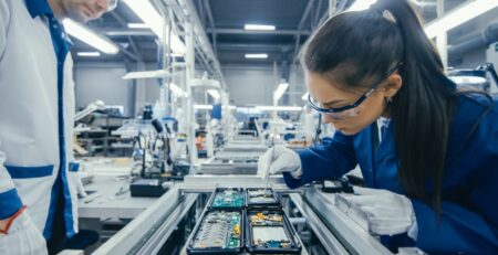
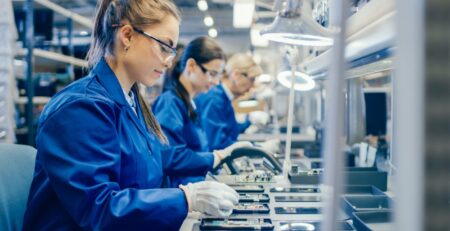
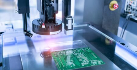
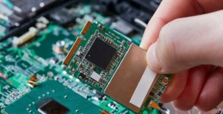
4. Printed Circuit Board Assembly (PCBA)
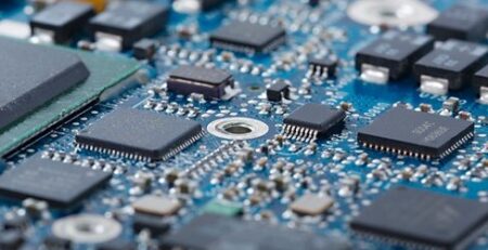
Once the board is fabricated, it enters the printed circuit board assembly (PCBA) phase. Components are mounted onto the board using either Surface Mount Technology (SMT) or Plated Through-Hole (PTH) techniques. Soldering, inspection, and quality testing ensure each component is correctly placed and functioning as intended.
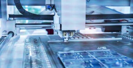
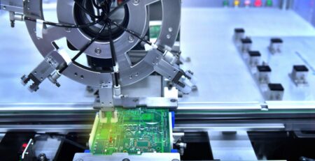
5. Testing and Quality Control
SVTronics employs a comprehensive range of inspections to verify board integrity and functionality. These include 3D solder paste inspection, Automated Optical Inspection (AOI), First Article Inspection, Flying Probe Testing, and In-Circuit Testing. We also ensure compliance with industry standards such as IPC 610 and ISO 9001, giving customers complete confidence in product reliability.
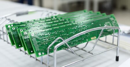
6. Final Packaging and Fulfillment
After passing all quality control checks, the assembled PCBs are carefully packaged and prepared for shipment. SVTronics offers full order fulfillment services, helping customers manage inventory, logistics, and delivery.
From Concept to Completion—SVTronics Is Your PCB Lifecycle Partner
The lifecycle of a printed circuit board involves far more than design or assembly—it’s a complex, multi-phase process that demands precision, expertise, and coordination. SVTronics supports customers at every step, offering flexible, high-quality, U.S.-based solutions that meet the demands of today’s most advanced technologies.
Whether in the prototyping phase or scaling for production, our team is ready to help you bring your next innovation to life.
Leave a Reply