The field of PCB manufacturing is expanding fast and the need for smaller and flexible computing solutions is on the rise. There is an increasing demand for digitalization in industrial and consumer electronics. The automotive and communications industries are driving innovations in PCB manufacturing along with technologies like AI and IoT.
The process of PCB manufacturing is often outsourced to a contract manufacturer (CM) who follows the designer’s plans. Those plans include a layout strategy, what kind of PCB substrate to use, and other requirements that must be decided before manufacturing begins. To improve your PCB manufacturing process, it is important to stay up to date with notable PCB trends in 2022.
High-Powered Boards
The demand for high-powered boards is growing. Modern devices require high-powered boards to work properly and their use is growing in many sectors. These boards are often made of heavy copper; they can handle higher currents, work longer, and resist higher temperatures than regular PCBs. In addition, due to their size, these boards allow for lighter, thinner, and more durable devices.
Benefits include:
- Resists temperature fluctuation
- Endures higher currents
- Lighter devices due to smaller size
Applications include:
- Industrial
- Military
- Aerospace
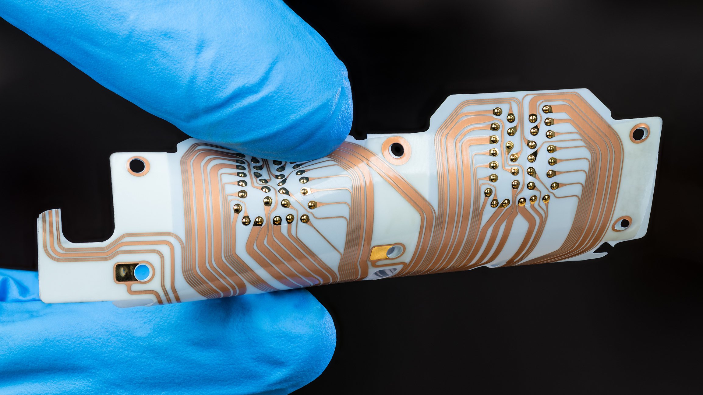
Flexible PCBs
Flexible PCBs, also known as flex prints or flex circuits, were created to allow for smaller mounting devices and have changed electronics’ shape and size, making them smaller and lighter. Modern manufacturing techniques have allowed for single-sided, rigid, and multilayer flexible PCBs.
Benefits include:
- Smaller than traditional PCBs
- More reliable and durable in harsh environments due to their temperature range
Applications include:
- Climate control, backup cameras, and navigation in the automotive industry
- Smart devices, medical equipment, scanners, and many more
High-Density Interconnect PCBs
A high-density interconnect PCB, or HDI PCB, refers to a circuit board with a high wiring density. HDI PCBs have many benefits, which explains their growing popularity in multiple applications and sectors. A higher wire density can save space by allowing the same number of connections in a smaller footprint. It can also decrease power consumption and boost battery life. With fewer layers and an increased transmission signal speed, HDI PCBs crunch more processes into a lighter board.
Benefits include:
- Smaller, lighter, and more reliable in harsh environments
- A blend of blind vias, buried vias, and micro vias to optimize for space
- Better signals than traditional PCBs
- Cost-effective for manufacturing
Biodegradable PCBs
Many industries are shrinking their environmental footprint and making choices in materials that are friendly to the planet. With 50 million tons of electronic waste produced worldwide each year, electronic waste is a serious issue that many manufacturers are thinking about.
The majority of electronic devices have a short lifespan, meaning they get used for a short period of time and then discarded as waste. That waste buildup causes environmental problems, as traditional PCBs can release toxins. Many manufacturers are now offering more environmentally friendly solutions with biodegradable PCBs. Since they’re made from natural materials such as wheat gluten, bananas, or even bird feathers, they can break down in water within 10 minutes. Many manufacturers offer both fully and partially biodegradable PCBs.
Learn more about how to minimize PCB waste.
Autoplacers With Automation
This PCB automation process is how the circuit manufacturers keep up as design technology progresses. Autoplacers are significantly more efficient than manual placement, and mass production of PCBs would not be possible without them. Automating these autoplacers is the next step for the industry. An automated autoplacer decides which component to place based on size and has the potential to speed up the manufacturing process. It’s even more efficient than its alternative, a PCB autorouter. In the future, this technology will seamlessly integrate with CAD systems to increase simulation speed significantly.
Are Your PCBs Fit for the Future?
PCB manufacturing is evolving rapidly to meet the needs of many sectors. With many breakthrough design innovations introduced by manufacturers, PCBs will be fit for almost all devices and industrial applications. Staying up to date on how the process works and understanding the latest trends will help you optimize your PCB technology and be ready for the future.
To find the help, consider working with an electronic manufacturing service for all your PCB needs.